
OKBNeftegazdiagnostika
Contact us ↗RU

Electronics and software

PCB design

Schematics, PCB layout and manufacturing documentation.

Purpose and approach

We design PCBs for instruments, measurement modules and control systems.
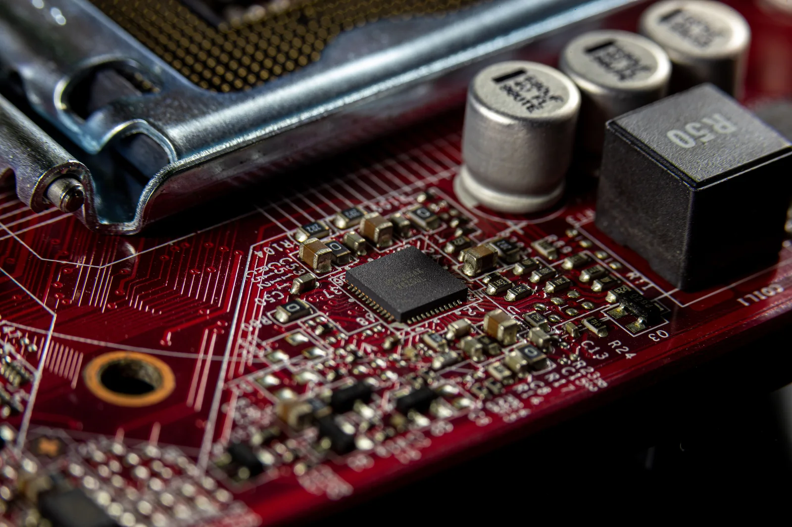
Electronic components on printed board
Electronic components on printed board · illustrative photograph · Sergei Starostin / Pexels

Work stages

  1. 01We agree on the board functions, supply voltages, connectors and enclosure constraints.
  2. 02We design the schematic, select components and verify their footprints.
  3. 03We place the components and route the board, then prepare the manufacturing files and bill of materials.
  4. 04For prototype orders, we test the power supply and board interfaces in the assembled instrument.
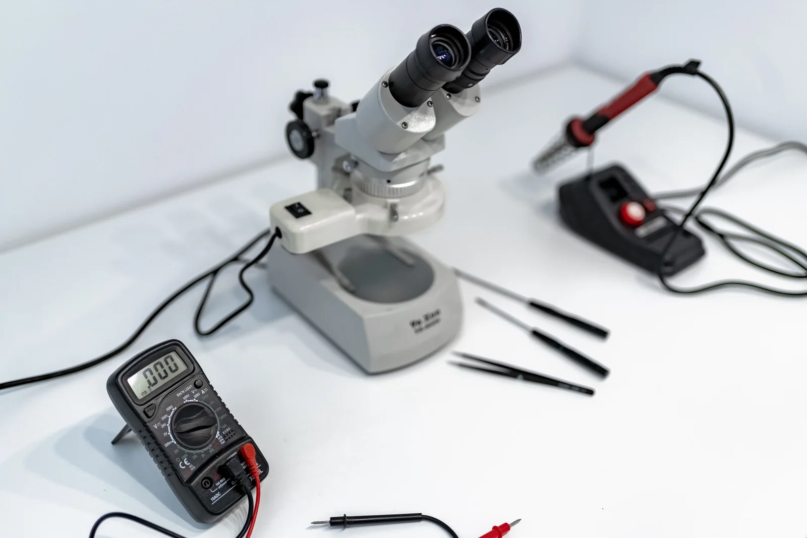
Microscope and electronic tools
Microscope and electronic tools · illustrative photograph · IT services EU / Pexels

To start work

What data will be needed

Feeding functions, power, interfaces, dimensions, operating conditions and expected output volume.

Contact OKB

Discuss a project

Describe the task and the materials you already have. You can email us additional files or a larger drawing.

work@okbngd.ru+7 (495) 233-59-59

Moscow. Please arrange visits and equipment handovers in advance.

Contact an engineer

PCB design

One PDF, DWG or JPG file, up to 2 MB.Privacy policy